Generic R&D
Enhanced Lateral Drift (ELAD) sensors
Vertex detectors at future linear colliders are required to feature a position resolution of about 3 μm in combination with a time resolution of down to 5 ns, while their thickness is limited to about 50 μm. This unprecedented combination of requirements is addressed by a new sensor concept developed by the DESY CMS group. The sensor bulk features a non-homogeneous lateral electric field, resulting in a position-dependent charge sharing. By this means, the spatial resolution of the impact position of ionising particles is greatly improved compared to standard planar sensors.
The spatial resolution of the impact position of minimum ionising particles (MIP) is usually improved by miniaturising the pixel or strip pitch of a sensor. The pitch describes the distance between two readout entities, and smaller pitches allow for a more precise measurement of the impact position. Additionally, a non-perpendicular incidence of the MIP or a strong magnetic field can render a higher resolution possible. However, these methods fail for sensors with a thickness below about 100 μm.
If the charge produced by a MIP in the sensor is collected by two readout entities, the impact position can be interpolated more precisely. Following this approach, the DESY CMS group has developed a dedicated charge-sharing mechanism that acts inside the sensor bulk. The ELAD sensor concept is realised by local modifications of the electric field in the sensor bulk, yielding a position-dependent charge collection at two electrodes. This approach is also feasible for thin detectors down to 50 μm thickness.
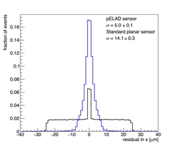
The buried implants form a p-n-p structure creating a lateral electric field component that influences the path of the charge carriers along their drift to the readout entities. The buried implants are sandwiched between epitaxially grown layers of silicon. Using Monte Carlo simulations, the resolution of ELAD sensors is evaluated as the root mean square of the difference between the true position and the interpolated position. At a pitch of 55 μm, the ELAD sensor shows an almost three times better position resolution than a standard sensor.ELAD sensors yield a narrower residual distribution than standard sensors and hence feature an improved position resolution (see Fig.1).
A dedicated production process was developed at Fraunhofer EMFT in Munich, Germany. The ELAD project is completely prepared for the production, which will take place shortly.
Compact Muon Solenoid Experiment
Enhanced Lateral Drift (ELAD) sensors
Vertex detectors at future linear colliders are required to feature a position resolution of about 3 μm in combination with a time resolution of down to 5 ns, while their thickness is limited to about 50 μm. This unprecedented combination of requirements is addressed by a new sensor concept developed by the DESY CMS group. The sensor bulk features a non-homogeneous lateral electric field, resulting in a position-dependent charge sharing. By this means, the spatial resolution of the impact position of ionising particles is greatly improved compared to standard planar sensors.
The spatial resolution of the impact position of minimum ionising particles (MIP) is usually improved by miniaturising the pixel or strip pitch of a sensor. The pitch describes the distance between two readout entities, and smaller pitches allow for a more precise measurement of the impact position. Additionally, a non-perpendicular incidence of the MIP or a strong magnetic field can render a higher resolution possible. However, these methods fail for sensors with a thickness below about 100 μm.
If the charge produced by a MIP in the sensor is collected by two readout entities, the impact position can be interpolated more precisely. Following this approach, the DESY CMS group has developed a dedicated charge-sharing mechanism that acts inside the sensor bulk. The ELAD sensor concept is realised by local modifications of the electric field in the sensor bulk, yielding a position-dependent charge collection at two electrodes. This approach is also feasible for thin detectors down to 50 μm thickness.
The buried implants form a p-n-p structure creating a lateral electric field component that influences the path of the charge carriers along their drift to the readout entities. The buried implants are sandwiched between epitaxially grown layers of silicon. Using Monte Carlo simulations, the resolution of ELAD sensors is evaluated as the root mean square of the difference between the true position and the interpolated position. At a pitch of 55 μm, the ELAD sensor shows an almost three times better position resolution than a standard sensor.ELAD sensors yield a narrower residual distribution than standard sensors and hence feature an improved position resolution (see Fig.1).
A dedicated production process was developed at Fraunhofer EMFT in Munich, Germany. The ELAD project is completely prepared for the production, which will take place shortly.
